Good Layout vs Bad Layout
- Gaurang Rane
- Nov 18, 2021
- 4 min read

In this experient, I designed a board to demonstrate good layout and bad layout for the effects of the switching noise.
This board will demonstrate 2 key features in layouting the PCB for reducing switching noise.
Continous return path under the signal traces.
Placement of decoupling capacitor close to the IC power pins.


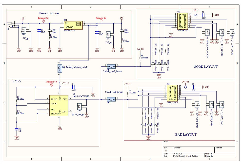
Circuit Design

Blocks -
5V Block – Takes input power from either Arduino or AC mains to 5V adapter.
LDO Block - Converts input 5V to 3.3V
IC 555 Block – Generates fast rise time signal. This signal is input to hex inverter circuit.
Good Layout Block – Routing is performed accordance with best design practices – Bottom layers has uniform ground layer; Decoupling capacitor is placed near to VCC pin of the IC.
Bad Layout Block – Layout contains many flawed trace routing and placement.
In this board, I am using IC 555 output as a clock and 2 hex inveter circuits. One circuit designed using best design practices and in the another region, same circuit but with very bad design practices.
The timer signal will connect to two different 7414 hex inverter chips. In each chip, there are 6 inverters. An inverter flips the input level to the output level. A LOW input creates a HIGH output. These 6 inverters in each chip are independent.
Three of the output signals from the hex will drive red LEDs with series resistors to limit the current. These will generate the dI/dt for the signal cross talk and the power rail noise.
Two of the inverters are special.
When the input to one is tied to 3.3 V. This means its output is always a low. The actual transistor level circuit for one inverter is shown below:
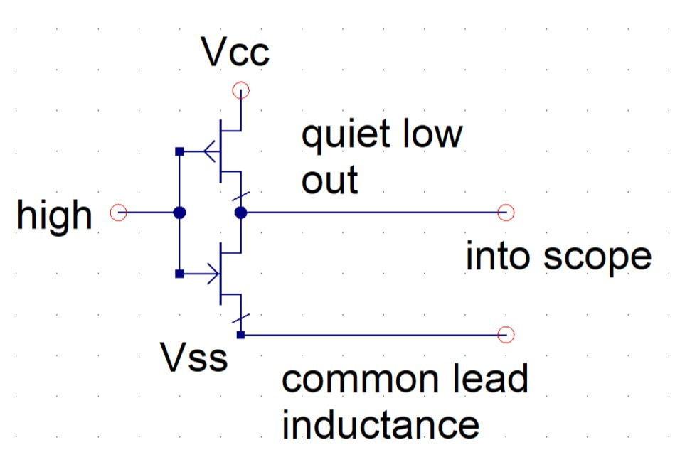
When the input is a high, the p-channel MOSFET connecting the output pin to the VCC rail on the die is open and the n-channel MOSFET on the low side is shorted. This connects the output pin to the Vss rail on the die.
When I measure the voltage on the output pin on the board, with the 10x probe, I am measuring the voltage of the output pin, relative to the local ground on the board. If there is any ground bounce noise from the local ground where the 10x probe is to the Vss rail on the die, it will appear as a voltage on the probe. This is how I measure ground bounce noise or cross talk between the quiet output signal-return loop that is not switching and the other signal-return loops that switch.
Likewise, a quiet HIGH output connects the output pin to the internal VCC rail on the die. This allows me to measure the switching noise on the power rail when the other I/Os switch.


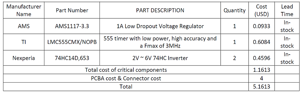
Non-commodity Components Bill of Material
Metrics to determine board is working
Stable 5V is observed on the TP1. LED1 is glowing.
Stable 3.3V is observed on the TP5. LED2 is glowing.
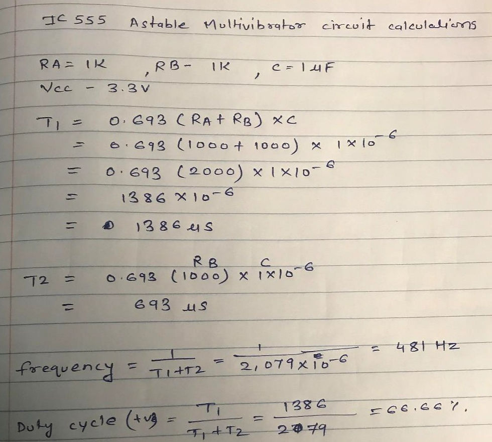
IC 555 frequency and positive duty cycle of the output in unloaded condition should be closer to expected results as per calculation.
Output at Q_Low_Bad & Q_Low_Good should be logic 0.
Output at Q_HI_Bad & Q_Hi_Good should be logic 1.
Risk assessment and Risk reduction features
Minimized unique component count- Capacitors and resistors
Reused the timer resistors capacitor circuit for 500hz/ 66% positive duty cycle.
Used mostly 1206 package resistors.
Used qualified parts to avoid footprint mismatch or incorrect footprint.
Debugging features on the Board
Switches on the board to isolate functional blocks and test them individually and sequentially.
LEDs are on the board to visually indicate state of the corresponding functional block.
All power traces are of width of 20mil. This makes identifying power traces easier.
All vias on the board are untented and far from the solder pads. All such vias acts as a test points.
Test points are present on the board to measure critical signals.
Bring-up plan for the board
Visually inspect the assembled PCB board.
Check the resistance between power and ground.
Check for continuity for the critical traces – (e.g. – trace connecting 3.3V to VCC of the ic)
Test functional block sequentially – (power -> IC555->Hex inverter)
Measurement and Analysis of the Signals
Power Signals
Stable 5V signal is observed at power supply input side.

Stable 3.3V signal is observed at LDO output.
IC 555 Output Characteristics
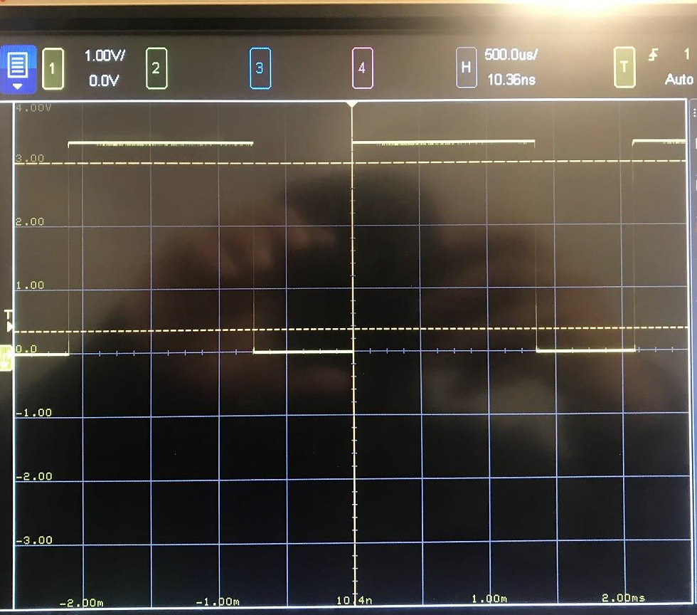
A. Measured frequency – 477Hz
B. +ve duty cycle – 67%
C. Voltage peak to peak – 3.29V
Hex_GOOD_OUT signal –


Rise time of the signal is 22.768ns and Fall time is 26.73ms. This signal is used for triggering to measure crosstalk and switching noise. Switching noise is synchronous with this signal.
Hex_GOOD_OUT and Hex_BAD_OUT signal rise time comparision
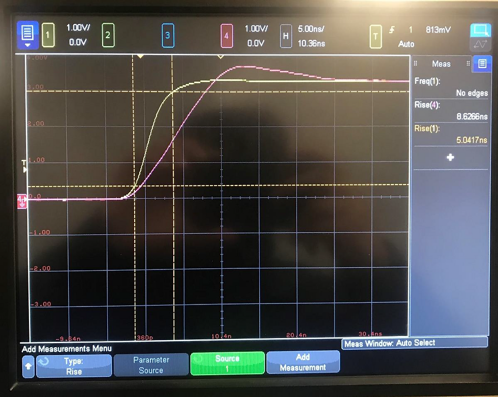
Good layout provides fast rise time of the signal because of low inductance in the loops.
Good layout measurement

Decoupling capacitor is placed near to IC VCC pin.
Common uninterrupted return plane is present on the bottom layer.
Q_LOW_GOOD measurements -

Red arrow denotes switching signals loop.
Yellow arrow denotes Q _LOW_GOOD loop.
Majorly Crosstalk happens inside the IC package.
Noise observed on the Q_LOW_GOOD is due to the layout.

Switching noise on Q_LOW_GOOD Vpk-pk = 86mV
Q_HI_GOOD measurements -

Switching noise on Q_HI_GOOD Vpk-pk = 132mV.
This switching noise depends upon placement of the decoupling capacitor.
Crosstalk also happens inside the IC package. This also contributes to the switching noise.
Bad layout measurement

Decoupling capacitor is placed far from IC. Large loop inductance is present between decoupling capacitor and IC.
Only one small width common trace is used as a return path.
Q_HI_BAD measurements -

Switching noise on Q_HI_BAD Vpk-pk = 784mV.
Q_LOW_BAD measurements -

Switching noise on Q_LOW_Bad Vpk-pk = 198mV
Conclusion
Switching noise and crosstalk is less if we follow good layout and component placement practices.
Good layout practices – Common ground plane at the bottom layer for return
Good placement practices – Place decoupling capacitor close to ic.
Route fast rising signals as short as short possible. Longer traces increases rise time due to inductance.
Recommendations
Place decoupling capacitor near to supply pin of the IC.
Use common uniform return plane.
Use 20 mil power traces even if current requirement is low. This will help in debugging process.
Use untented via away from solder pads in initial prototypes. This vias acts as potential test points.
Use qualified parts to avoid problems such footprint mismatch.
Reuse earlier used and tested design.
Minimize unique part count to minimize risk mitigation of assembly procedure issues.
Comments